
 Audit hochschule und familie

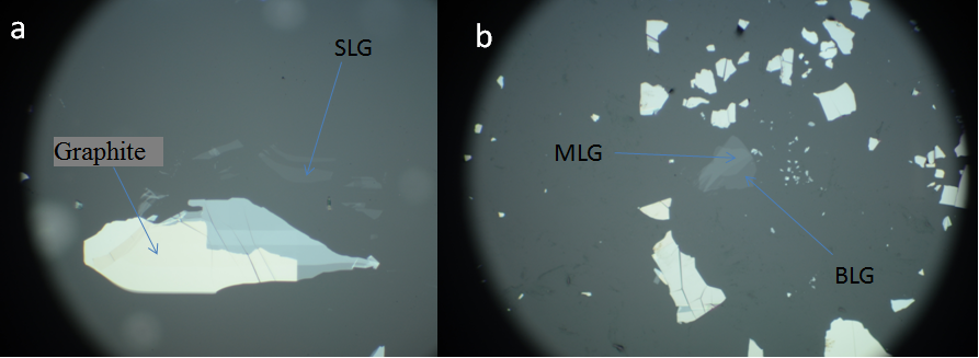
Figure 1: (a) Single layer graphene (SLG) has less that 5% contrast differences with PMMA
(b) Bilayer graphene (BLG) and Multilayer graphene (MLG)
Position Indication:
Content

2013 - Sajjad Tollabimazraehno
Capacitive Imaging Technique in UHV-STM to Find Graphene Flakes
Tip Ultra High Vacuum (UHV) Scanning Tunneling Microscopy (STM) to Find Micron Size Graphene Flakes on
Boron Nitride (BN)
Research stay at the University of California, Berkeley, USA
15/04/2013 - 30/09/2013
Sajjad Tollabi
Contact: vorname.nachname(/\t)jku.at
Graphene device preparation
The sample was a single layer of graphene on Boron Nitride (BN) on SiO2. The BN layer which has almost the same lattice constant as graphene, were transferred by exfoliation process onto SiO2. Silicon wafer has a thermal oxide of Si on both sides with a thickness of 270nm. After transferring of BN, the graphene flakes were transferrred in a process called "Dry Transfer" (Fig.1). Finally, some Au/Cr electrodes were evaporated onto graphene after structuring them by electron lithography (Fig.2) in order to do the transport measurement inside the UHV-STM.
This h-BN crystal has the hexagonal lattice parameter close to graphene and strong ionic bonds in lattice plane. h-BN is relatively inert and the planar surface suppresses rippling and wrinkles in graphene [1, 2] and is free of dangling bonds and surface charge traps [3]; therefore, the graphene flake on h-BN is free of distortions and wrinkles. A sharp metallic tip scans the sample surface and records the surface topography as a function of tunneling current, which depends exponentially on the tip-sample distance, by applying a voltage between tip and sample in a scanning tunneling microscope (STM)[4]. Therefore, it is not possible to scan non-conductive surfaces. The graphene flake is placed on an insulator material with 10 micrometer size. The only conducting material is the graphene flake, which is even smaller than theh-BN and is too small to be found. One needs a coarse walker stage for tip navigation parallel and perpendicular to the sample surface that can follow the wires by traveling in millimeter distances and change the tip-sample distance. The capacitance current is proportional to the inverse tip-sample distance. The capacitance current, proportional to inverse of tip-sample distance, cannot be used to find the electrode edges at higher distances. Therefore, in each step, we have to approach the tip to tunneling regime and retract it. The smaller working distance is not favorable due to the risk of tip crashing at high speed scanning although at higher working distance the resolution of edge detection is low, so, for a narrower wire it is important to have the lower working distance. We used the long focus optical microscope to find the largest gold electrode as a starting point for navigation.
Wire edge detection
As the tip moves across the micron size gold wire, the variation of the capacitance current (when the tip is far enough that it is not in tunneling mode so that we have only capacitance current) was plotted as a function of tip steps which correspond to the tip traveling distances. In Fig.3 the pickup current I and its spatial first derivative dI/dx are shown. The two turning points in the first derivative correspond to the gold wire edges. The sharpness of the turning points decreases with increasing tip-sample distance and is getting blurred (more round and broader). However, to have a good resolution in the edge detection, the tip-sample distance should be comparable with the wire's width. Therefore the distance/width ratio should be less than 0.3 to permit an accurate edge identification. When the features become smaller, it is important to approach the tip to tunneling regime and retract it to obtain the desired resolution.
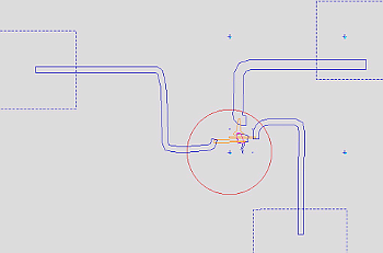
Figure 2: Electrodes and wires, the pink area is the graphene flake and micron size
wires to make connection with the external system for the measurement of its transport properties
Navigation protocol
First of all, we have to find the largest gold contact and approach the tip next to the thinner wire which is connected to the plate, then retract the tip to a height corresponding to an aspect ratio of 0.3 and phase lock it in lock-in amplifier. The main point is to identify the center of the electrode from the spatial derivative of the capacitance current and move the tip along the gold wire to reach the graphene. After phase lock, the tip was moved towards the thinner wire and the capacitance current was recorded as a function of the number of tip steps when the program controls the tip to move across the wire. In order to identify the center of the wire (between the two turning points in the first derivative) the length of the scanning line must be at least twice the wire width. We then move the tip to the center of the wire and approach it. Typically the substrate is not perfectly horizontal; therefore, the tip can crash during navigation. To avoid crashing, it is better to approach the tip and retract it again to be sure that the tip will not crash, after each edge detection. Sometimes the width of the graphene flake is so small or the two electrodes on graphene are so close to each other that they interfere on capacitance measurements. In this case, it is better to have different widths for electrodes to make a good contrast when searching for the graphene sample. Figure 4 shows the Moiré pattern of graphene on BN after finding micron size graphene flake on insulator.
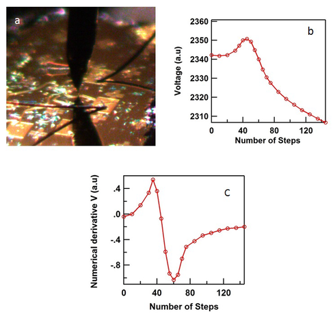
Figure 3: Variation of the capacitance current as the tip moves across the gold wire:
(a) distance/width ratio less than 0.3, tip scanning the wire
(b) capacitance current converted to voltage in each tip step across the wire
(c) first derivative of capacitance current dI/dx, the tow turning points correspond to the wire edges
(a) distance/width ratio less than 0.3, tip scanning the wire
(b) capacitance current converted to voltage in each tip step across the wire
(c) first derivative of capacitance current dI/dx, the tow turning points correspond to the wire edges
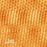
Figure 4: Scanning tunnelling microscopy (STM) image of graphene on Boron Nitride (BN).
The Moiré pattern (the large scale superstructure) is the result of the superposition of the graphene lattice
with the lattice of BN, and the small dark spots are the centers of carbon rings. The
image size is 5nm X 5nm; Tunneling parameters are I = 436 pA and V = -200 mV.
[1] Chun Hung Lui, Li Liu, Kin Fai Mak, George W Flynn, and Tony F Heinz. Ultra graphene. Nature 462 (7271) : 339 {41, November 2009}. doi: 10.1038/nature08569. http://www.ncbi.nlm.nih.gov/pubmed/19924211.
[2] Masa Ishigami, J H Chen, W G Cullen, M S Fuhrer, and E D Williams. Atomic structure of graphene on SiO2. Nano letters 7 (6):1643 {8, June 2007}. doi: 10.1021/nl070613a. http://www.ncbi.nlm.nih.gov/pubmed/17497819.
[3] C R Dean, a F Young, I Meric, C Lee, L Wang, S Sorgenfrei, K Watanabe, T Taniguchi, P Kim, K L Shepard, and J Hone. Boron nitride substrates for high-quality graphene electronics. Nature nanotechnology 5 (10) : 722 {6, October 2010}. doi: 10.1038/nnano.2010.172. http://www.ncbi.nlm.nih.gov/pubmed/20729834.
[4] G. Binning, H. Rohrer, Ch. Gerber, and E. Weibel. Surface studies by scanning tunneling microscopy. Phys. Rev. Lett. 49 : 57 {61, Jul 1982}. doi: 10.1103/PhysRevLett.49.57. http://link.aps.org/doi/10.1103/PhysRevLett.49.57.
[5] Guohong Li, Adina Luican, and Eva Y Andrei. Self-navigation of a scanning tunneling microscope tip toward a micron-sized graphene sample. The Review of scientific instruments, 82(7) : 073701, {July 2011}. doi: 10.1063/1.3605664. http://www.ncbi.nlm.nih.gov/pubmed/21806183.
[6] Stuart B. Field and John Barentine. Capacitive position sensor with simultaneous, linear X-Y readout. Review of Scientic Instruments, 71(6) : 2603, 2000. doi: 10.1063/1.1150656. http://link.aip.org/link/RSINAK/v71/i6/p2603/s1&Agg=doi.